Adesis
Alloy Sputtering Targets
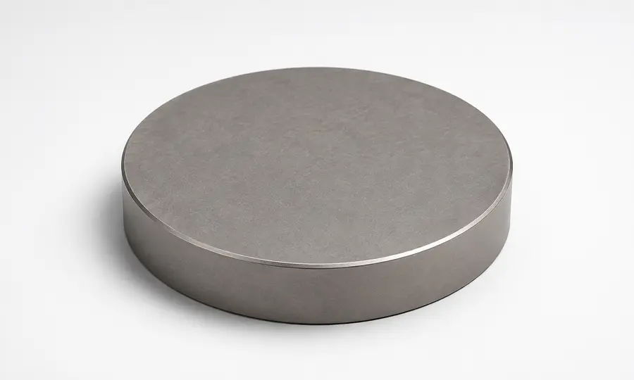
An alloy sputtering target is a piece of metal that is made up of a mixture of two or more elements.
High-purity crystal / semiconductor
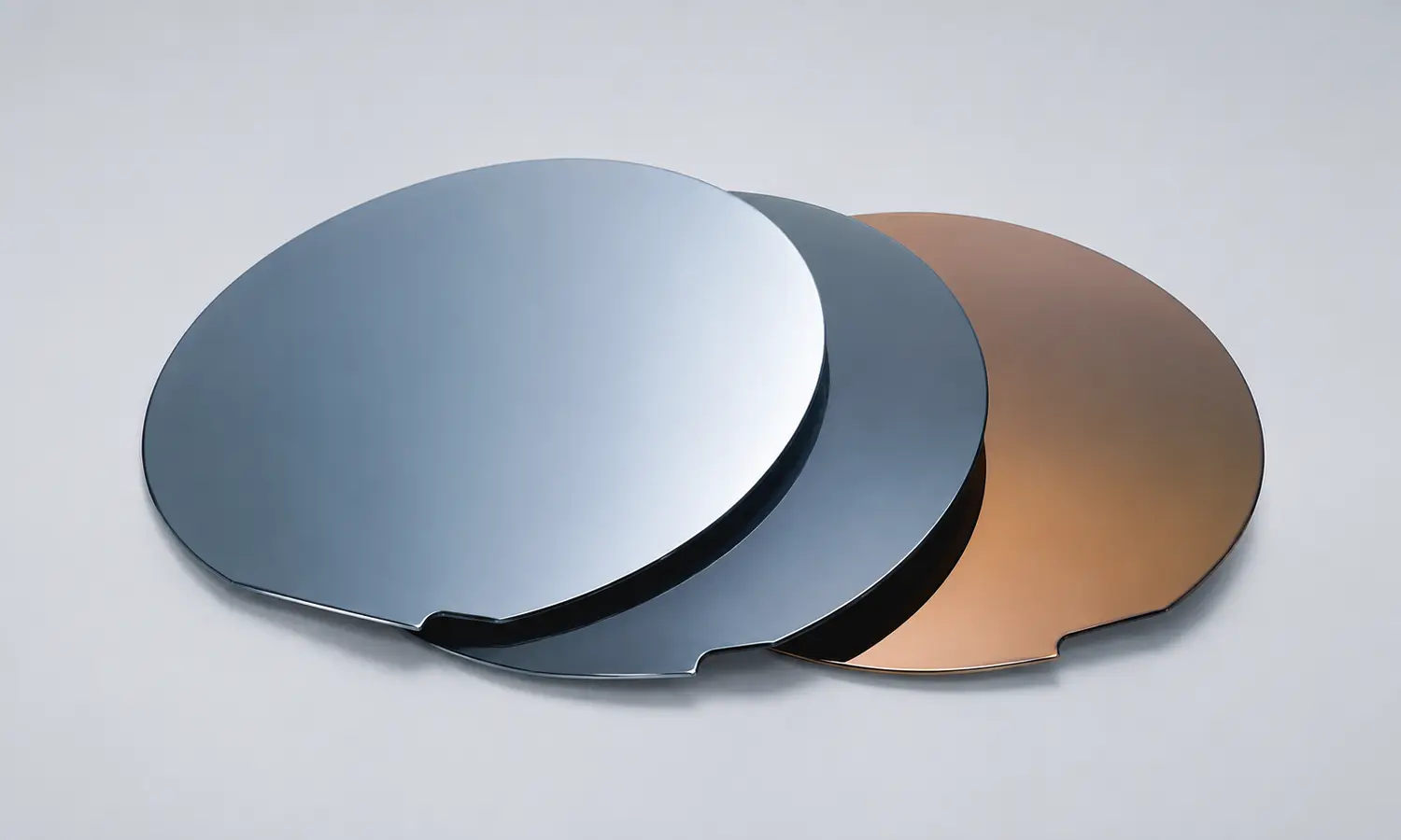
Semiconductor Wafers & Substrates
High-purity crystal / semiconductor
Silicon carbide (SiC) wafer is a semiconductor material that is used in the production of electronic and optoelectronic devices. SiC wafers are thin, circular discs of SiC that are used as a substrate material in the manufacturing of these devices.
SiC is known for its high thermal conductivity, high electron mobility, and high breakdown voltage, which make it useful in a variety of high-power and high-temperature applications. It is used in the production of transistors, diodes, and other electronic devices that are capable of operating at high power levels and high temperatures.
Adesis
An alloy sputtering target is a piece of metal that is made up of a mixture of two or more elements.
Adesis
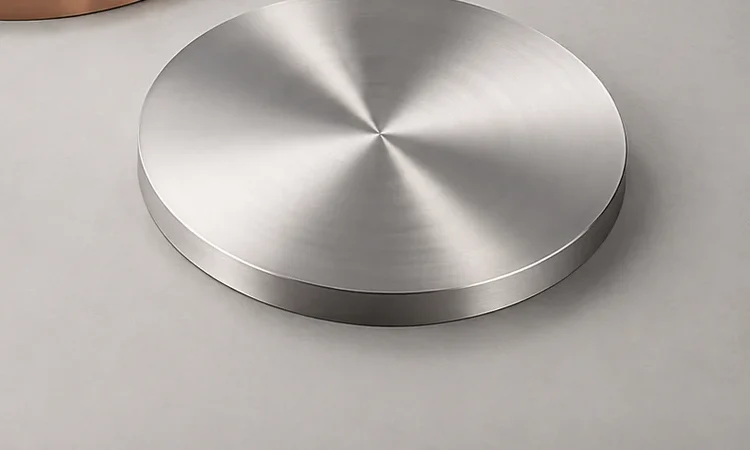
A pure metal target is a piece of metal that is composed of a single element or compound, rather than being an alloy made up of multiple elements.

Adesis
A compound sputtering target is a piece of material that is made up of two or more elements combined in a specific chemical formula.
Yes. The Silicon Carbide (SiC) Wafers is available in Turkey through ZENOTEK, Adesis’s distributor.
ZENOTEK prepares a project-specific quote for every request; add the product to your quote list and request pricing with a single form.
High-purity crystal / semiconductor