Adesis
Silicon Carbide (SiC) Wafers
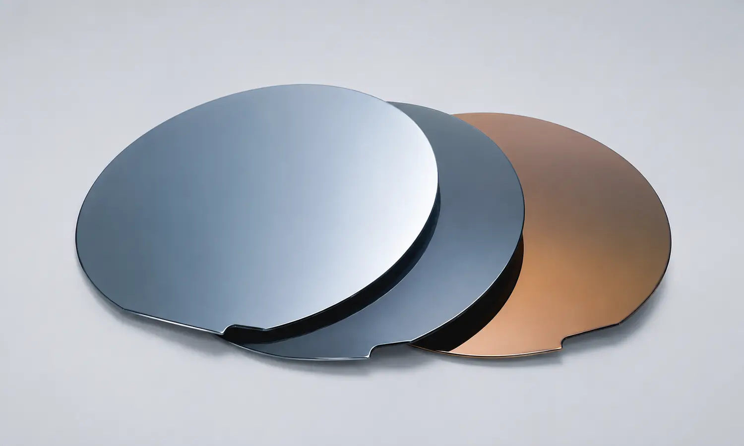
Silicon carbide (SiC) wafer is a semiconductor material that is used in the production of electronic and optoelectronic devices.
High-purity crystal / semiconductor
Materials & Substrates
PVD sputtering targets, evaporation materials, MBE sources, rare-earth metals, technical ceramics, conductive glass and high-purity Si, SiC, GaN and GaAs wafers.
Showing 9 of 406 products
Adesis
Silicon carbide (SiC) wafer is a semiconductor material that is used in the production of electronic and optoelectronic devices.
Adesis
Silicon wafer are an essential component in the production of a wide range of electronic devices, including computers, smartphones, and other consumer electronics, as well as industrial and medical devices.
Adesis
A thermal oxide silicon wafer is a silicon wafer that has been coated with a layer of silicon dioxide, also known as silica or glass, using a process called thermal oxidation.
Adesis
Quartz, also known as silicon dioxide (SiO2), is a naturally occurring mineral that is commonly used as a substrate in a variety of applications.
Adesis
Gallium nitride (GaN) wafer is a semiconductor material that has a wide bandgap and a high breakdown voltage, making it suitable for use in high-power and high-frequency electronic devices.
Adesis
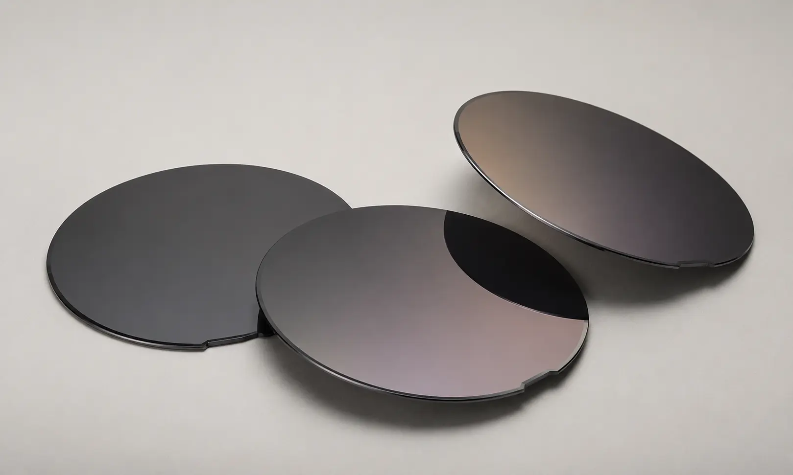
Gallium arsenide (GaAs) wafer is a semiconductor material that is used in the production of electronic and optoelectronic devices.
Adesis
Gallium antimonide (GaSb) is a semiconductor material that is used in the production of electronic and optoelectronic devices.
Adesis
Indium arsenide wafers supplied for infrared detectors, high-electron-mobility devices, quantum structures and III–V epitaxial research.
Adesis
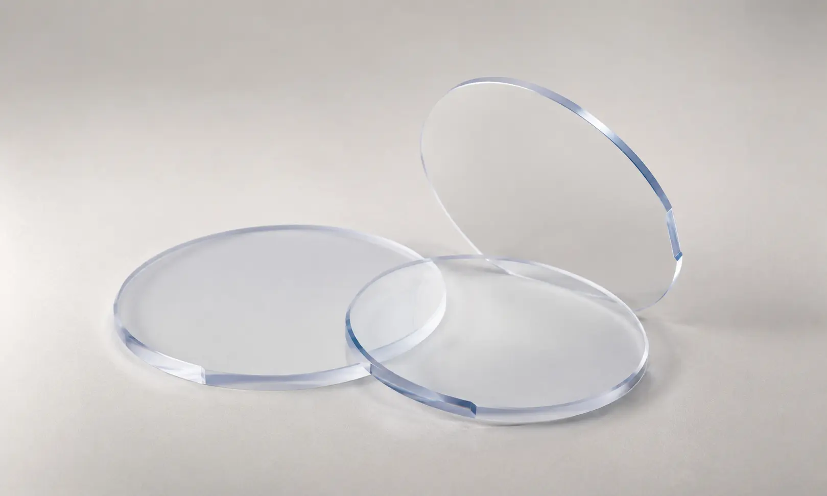
Single-crystal sapphire wafers for GaN epitaxy, optical windows, sensors and high-temperature device research.